
.JPG)
.JPG)
Portuguese National Electron Microscopy Network
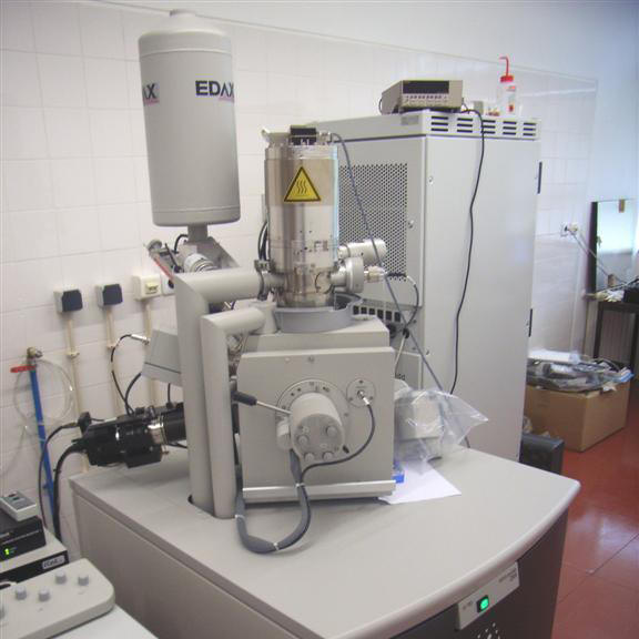
Ultra-high resolution field-emission Scanning Electron Microscope, with integrated microanalysis X-ray system (EDS - energy dispersive spectrometer) and Electron Backscatter Diffraction (EBSD)
Type of analysis:
The microscope allows the analysis of conductive, semiconductive and nonconductive samples including any type of polymer, metal, ceramic or organic material.
This ultra-high resolution microscope (<1.8 nm both at high and low vacuum) is particularly developed for the study and characterization of nanomaterials such as: diamond coatings, thin films; carbon nanotubes, nanoparticles, semiconductors, polymers, porous materials, glass substrates, organic materials, among others.
Additionally, the Nova NanoSEM 200 possess unique ultra-high resolution characterization capabilities in low vacuum, an environment that suppresses the charge on non-conducting materials or components and cancels self-contamination of the sample or contamination induced by the electron beam. Thus, it is especially designed for the analysis of charged and/or contaminated samples. This charge elimination also removes the need for applying conductive coatings that can obscure the image details and interfere with the compositional analysis.
With the integrated X-ray microanalysis (EDS) and the electron backscatter diffraction pattern detection and analysis system (EBSD), it is possible to perform acquisition and analysis of X-ray spectra from B to U. Additionally, we can obtain X-ray profiles maps by elements and perform sequence analysis of particles and regions in a sample. The EBSD system, allows the record and analysis of the backscattered electron diffraction patterns in a point or in a specific region of the sample.
Technical Specifications:
Integrated system (EDS - energy dispersive spectrometer /EBSD - Electron Backscatter Diffraction), EDAX- Pegasus X4M
High vacuum resolution
Low vacuum resolution
Electron beam resolution
Beam landing energy: 200V to 30 kV
High stability Schottky field emission gun with automatic operation
Probe current: 0.3 pA to 22 nA, continuously adjustable
Chamber vacuum (high vacuum): <10-4 mBar
Chamber vacuum (low vacuum): <2 mBar
Detectors:
Chamber:
Image processor resolution:
Pattern processor resolution:
Operation control:
Integrated Energy Dispersive Spectrometer (EDS) and Electron Backscatter Diffraction pattern (EBSD), EDAX- Pegasus X4M
EDS Specifications
Si (Li) detector - SEM ultra-thin window (SUTW) type;
Qualitative and quantitative acquisition and analysis of X-ray spectra (B-U) - with ZAF and FIROZ correction matrix;
Digital capture of SEM images and selection of the analysis point/region;
X-ray profiles maps by elements, full and quantitative spectrum;
Automated acquisition of X-ray maps into multiple regions;
Automated sequential analysis of multiple particles and regions/fields.
EBSD Specifications
EBSD detection unit with DigiView III camera and “Forward Scatter Detector System” detector;
Software for recording and analysis of the backscattered electron diffraction patterns in a point or in a specific region of the sample;
Software for recording, processing and analysis of IOM;
"Delphi Software" for phase identification, matching results of EDS and EBSD analysis (ICDD database- Version Academic).
.JPG)
.JPG)
The Managing and
Financing Entity
of the National Scientific
Re-equipment Program(PNRC):
FCTFCT -
Foundation for Science and
Technology
Project REDE/1511/RME/2005


|
|
NanoSEM - FEI Nova 200 (FEG/SEM); EDAX - Pegasus X4M (EDS/EBSD) |
![]()